Photonic Chips Factory In Eindhoven: Where Silicon Meets Light at Lightning Speed
Photonic Chips Factory In Eindhoven: Where Silicon Meets Light at Lightning Speed
At the heart of Eindhoven’s innovation ecosystem, a revolutionary facility is redefining the future of computing. The Photonic Chips Factory stands as a beacon of next-generation semiconductor technology, merging photonics with silicon to deliver ultrafast, energy-efficient data processing. Unlike traditional electronic chips, these photonic integrated circuits harness light instead of electrons, enabling data transfer at near-light speed with dramatically reduced power consumption.
This deep dive explores how this pioneering factory is transforming global technology demands—through precision engineering, sustainable design, and industrial-scale scalability. The facility, located in one of Europe’s tech innovation hubs, represents a strategic convergence of academic excellence and industrial prowess. Home to cutting-edge research and large-scale manufacturing, the plant operates at the intersection of photonics and microelectronics.
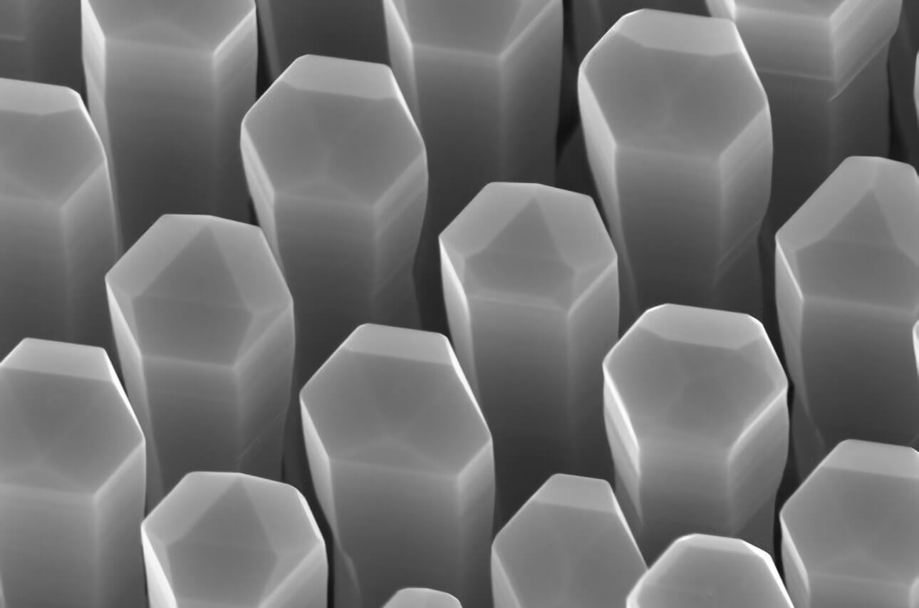
Photonic chips developed here exploit optical waveguides, modulators, and detectors fabricated using state-of-the-art nanofabrication processes. These components form intricate circuits that transmit and process information via photons—particles of light—offering bandwidth and speed unattainable by conventional silicon electronics.
Inside the Photonic Revolution: How Light Beats Electronics
Unlike traditional microchips that rely on electron flow, photonic chips leverage photons to move data across circuits, unlocking unprecedented performance.“Light doesn’t overheat, doesn’t degrade signal quality over distance, and transfers data at 50% faster rates,” explains Dr. Liesbet Bungers, a photonics expert collaborating with the Eindhoven facility. “This opens doors to applications ranging from quantum computing to real-time AI inference, where speed and efficiency are non-negotiable.” At the core of the factory’s operations are two principal innovations: - **Photonic Integrated Circuits (PICs):** Miniaturized optical pathways etched onto silicon wafers, combining optical components such as beam splitters, phase shifters, and detectors in a single chip.
These PICs enable complex signal processing for telecommunications, sensing, and high-performance computing. - **Hybrid Integration Techniques:** Seamlessly combining III-V semiconductor materials—like indium phosphide and gallium arsenide—with silicon photonics substrates. This hybrid approach enhances light generation, amplification, and control while leveraging existing silicon manufacturing infrastructure.
The production process integrates extreme precision lithography, atomic layer deposition, and wafer-scale testing. Each photonic chip undergoes rigorous performance validation to ensure signal integrity at terahertz frequencies—far beyond the reach of copper-based electronics. The result is a chip architecture capable of transmitting multiple terabits of data per second over compact form factors.
Sustainability and Scalability: Manufacturing at Industrial Scale
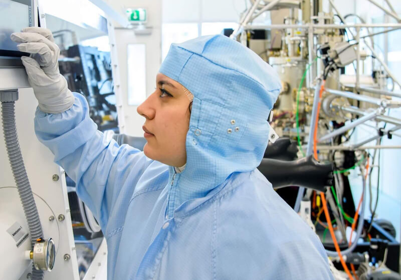
Beyond technological breakthroughs, the Eindhoven factory excels in sustainable, scalable manufacturing. Traditional semiconductor fabrication is notoriously energy-intensive and environmentally taxing. This facility redefines efficiency: by replacing electric-powered signal routing with photonic transmission, power consumption drops by up to 90% under peak loads.“Every watt saved at the chip level ripples through global data center energy demands—this is sustainability by design,” notes factory operations chief Tom Reisner. Scalability is embedded in the factory’s DNA. Using wafer-level manufacturing—processing hundreds of microchips simultaneously on a single silicon wafer—yields throughput rates that outpace conventional design.
Advanced automation and AI-assisted quality control ensure uniformity across batches, reducing waste and downtime. The plant employs a closed-loop water recycling system and renewable energy sources to further minimize its ecological footprint.
- Hybrid Material Integration: Combining III-V materials on silicon enhances light emission and optical gain critical for active photonic components.
- High-Speed Testing Protocols: Real-time optical coherence and signal integrity measurements validate chip performance before shipment.
- Modular Design Flexibility: Chips can be reconfigured for diverse applications—from high-frequency trading servers to edge AI devices—without full redesign.
Industry Impact: From Quantum Computing to Smart Cities
The photonic chips emerging from Eindhoven are already reshaping industries.In quantum computing, their low-loss optical interconnects enable stable qubit communication across quantum processors. For artificial intelligence, photonic accelerators process complex neural networks with minimal latency and heat—critical for real-time decision-making in autonomous systems. In telecommunications, the chips boost 5G and future 6G networks, enabling ultra-dense connected communities through faster, more reliable bandwidth.
Smart cities benefit as well. Sensor networks embedded with photonic chips deliver real-time environmental monitoring—air quality, noise levels, traffic flow—with energy budgets suitable for long-term deployment. No longer constrained by bandwidth bottlenecks, urban infrastructure evolves into responsive, data-rich environments.
Global tech leaders, including multinational semiconductor firms and cloud service providers, are already integrating these chips into pilot deployments. Early results show reduced latency, lower carbon emissions, and enhanced reliability—metrics reshaping procurement strategies worldwide.
Outlook: The Photonic Era Is Here
Eindhoven’s Photonic Chips Factory does more than produce advanced semiconductors—it accelerates the transition to a light-based computing paradigm.By merging fundamental physics with industrial innovation, it delivers tangible solutions to humanity’s growing demand for speed, efficiency, and sustainability. As Dr. Bungers frames it: “We’re not just building chips—we’re building the nervous system of the next digital age.” With continued investment and international collaboration, Eindhoven is poised to remain a global pioneer, illuminating pathways toward smarter, greener, and faster technology.
The future of computing is photonically powered, and Eindhoven stands at its forefront.


Related Post
FBI Operatives Honestly Admit They Can Never Unsee: Inside the Unbreakable Grief of Witnessing Unspeakable Narrative
Chipotle Opening Hours: When Can You Get Your Burrito Fix?
Psepseiimaderasese Shooting News Today: Where Firepower Meets Frontline Despair in Escalating Conflicts

Was Ynw Melly Found Guilty? The Controversial Verdict in the Legal Battle of the Decade